There are various methods for creating patterned electronic devices, many of which might be referred to as lithography.
With photolithography, a photo-responsive polymer – referred to as a photoresist – is coated onto the material (substrate) to be patterned. A mask can then be positioned above the substrate, which is exposed to a ‘flood’ of light (of a specific wavelength). The aim of the mask is to block light reaching the substrate so that a specific pattern of light has illuminated it. Alternatively, with maskless photolithography the pattern is projected onto the substrate. After this exposure, the substrate is developed in a solution chosen to dissolve unwanted resist, leaving the required pattern. This requires some calibration and control so that you can obtain uniform thickness of polymer across the substrate, and develop a fixed recipe with required exposure and development times.
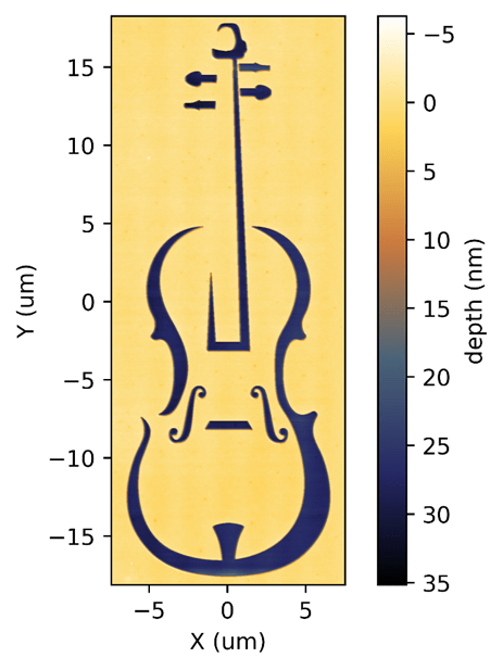
With the violins that we patterned whilst testing the new nanolithography system (combined Nanofrazor from Heidelberg Instruments and thin film deposition chambers) we used scanning probe thermal lithography instead. This has some advantages including removing the need for markers as underlying patterns can be detected using the scanning probe microscope itself.
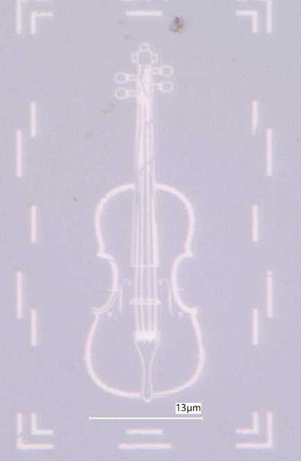
What we were aiming for was a simple bilayer pattern that could be created in one or two steps. This favours black and white images or line art. Of a selection of violins we chose the following two designs:

Where the strings could be added during the first pattern, or as an additional step. This was later modified to include a frame to assist lift-off of unwanted material and alignment of the violin body to the strings.
There were then a few different approaches that we tried, with the equipment that we had installed at the time: 1) Direct patterning into PPA; 2) Pt violin patterned in a single step; and 3) Multi-layer patterning (i.e. adding the strings on after patterning the first layer).
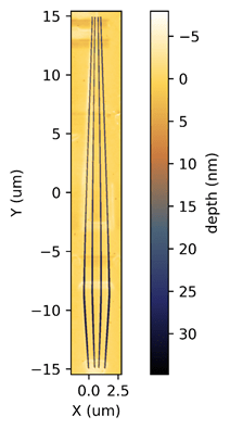
1) Direct patterning into PPA
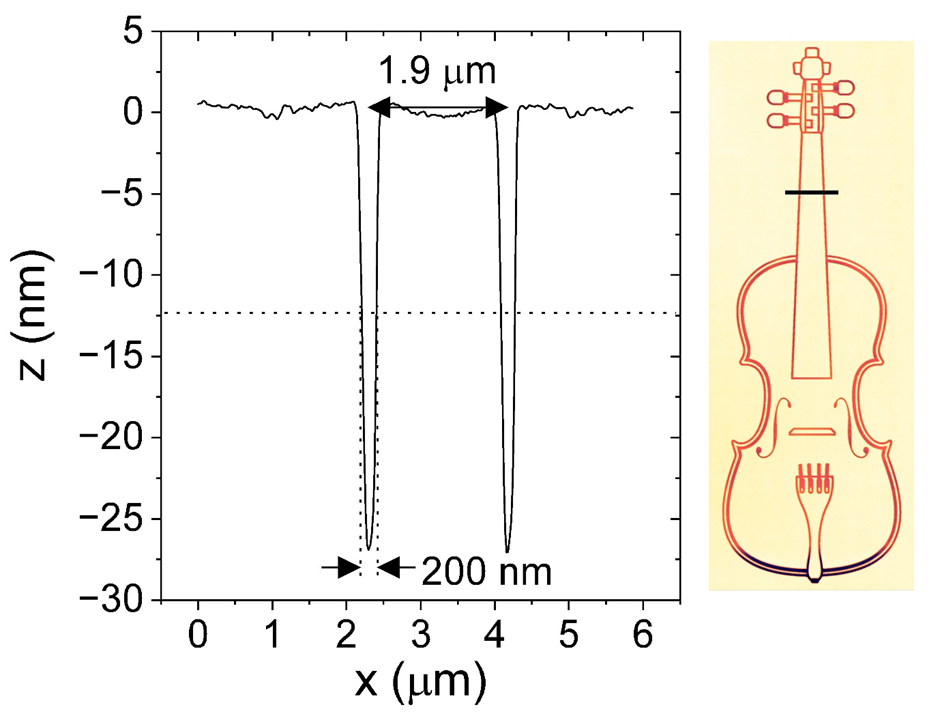
Whilst patterning the platinum violins required developing steps which limit the achievable resolution, we can directly pattern the image onto the thermal resist (PPA) with a minimum pixel size of 20 nm. To demonstrate this, we patterned ‘unstringed’ violins of the order of 3 micron wide with line features as small as 200 nm and a neck roughly 1.9 microns wide.
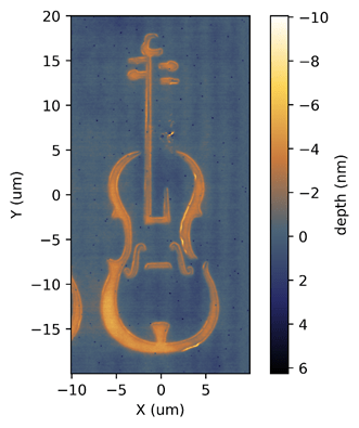
2) Pt violin patterned in a single step
For standard bottom-up patterning a bilayer resist stack is used, where the top thermal resist (PPA) is patterned by the Nanofrazor, and the bottom resist (underlayer) is etched away to expose the substrate that we want to attach our platinum violin to. For this approach the violin and strings are patterned in a single step followed by:
- Developing the underlayer in ethanol (glovebox friendly),
- Cleaning the exposed surface with argon ion milling,
- Deposition of Ti (for adhesion) and Pt using magnetron physical vapour deposition,
- Lift-off of unwanted material with acetone
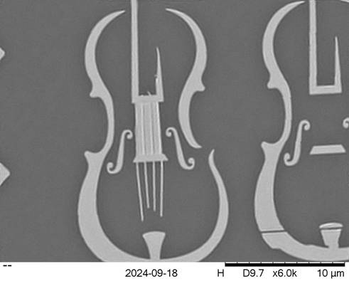
3) Multi-layer patterning (i.e. adding the strings on after patterning the first layer).
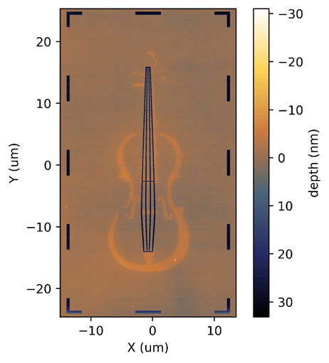
For creation of more complex devices, multi-step patterning is required. With other lithography techniques this requires a set of markers and alignment tools or procedures to ensure that the next pattern lines up well with the original. With the Nanofrazor, the scanning probe (cantilever) can read subtle changes in surface height of our substrate even if coated by our bilayer resist stack. This allows us to visually identify the area of interest and then precisely locate the original pattern that we wish to add to. In our case: strings to the violin body. Once this has been identified we can reorientate our pattern so that it aligns with the original structure:
Follow step 2, but without patterning strings:

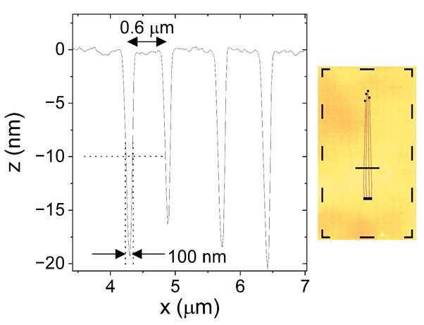
Note that the aim here was to have a neck that could accommodate 100 nm strings separated by a distance of at least 100 nm.
Re-clean and spin coat the polymer resists for patterning.
Find the original patterned violin using the Nanofrazor cantilever:

Align strings with the violin body and pattern over it:

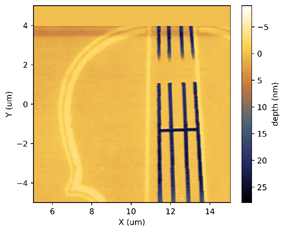
Then repeat steps from (2) (develop, descum, deposit, lift-off).
We tried a variety of string thicknesses, down to as thin as 100 nm. In principle we should be able to achieve 20 nm width (with a slightly different recipe) once we have our reactive ion etcher online.