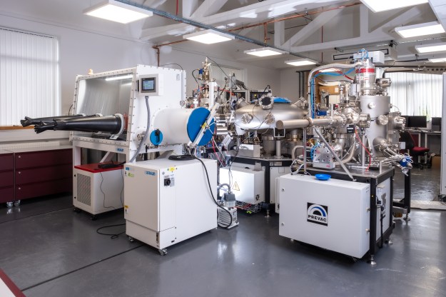
Nanolithography and thin film deposition system
Recently installed £2M Strategic Equipment from EPSRC. This multi-chamber system will enable thin film deposition by RF/DC sputtering and e-beam as well as thermal scanning probe lithography (Nanofrazor) and scanning probe microscopy (STM/AFM) all without exposing the sample to air.
See here for more on violin lithography as featured on TechNow.
Ar ion miller and Microwriter maskless photolithography
Class 100 clean room with maskless photolithography (resolution limit 600 nm), and argon ion milling available in Department. Training is required for use, however we can also provide patterned devices on arrangement. 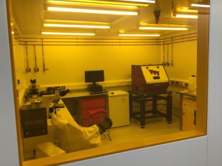
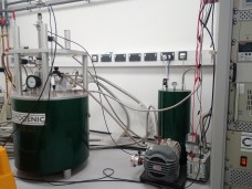
Cryogen-free magnetometer
Variable magnetic field (0-9T) and temperature (300mK – 400 K) for vibrating sample magnetometry (VSM), resistivity and thermal transport (thermal conductivity and Seebeck coefficient*) measurements.
*The Seebeck effect manifests as a generation of a current (voltage) when a temperature difference occurs between two junctions. This can be used to harvest energy but in order to develop new materials a measure of the Seebeck coefficient (how much voltage is generated per Kelvin) is required.
Magnetothermal Measurements
A relatively new phenomena – the spin Seebeck effect – manifests as the generation of a spin polarised current when a temperature difference is set up between two junctions of a magnetic material. This effect is of particular interest as it hints at the possibility of spin dependent thermal conductivities, a property that could lead to a breakthrough in energy harvesting technology. The measurement of this effect is possible by making use of the inverse spin Hall effect.
We have several sample holders designed to measure the spin Seebeck effect- from monitoring the temperature difference across a 10 mm wide sample, to large area (40 x 40 mm) sample holders with integrated Peltier cells to monitor the heat flux and temperature difference across the sample. We are also working with beamline scientists with STFC to develop an in-situ spin Seebeck measurement for neutron reflectometry.


Thin film transport measurements – 4 point probe
Utilising a Keithley 6221 current source and 2182 nanovoltmeter, Van der Pauw, Hall and Magneto-Resistance measurements are achievable with respect to magnetic field (~0-0.5 T) and temperature (~ 20-300 K). Fully automated and capable of resistances ranging from mOhms to 20 MOhms.
Magnetic measurements – Magneto-Optic Kerr Effect
Using the change in polarisation of light interacting with magnetic material (Kerr effect) to determine the coercive field of thin films. Capable of magnetic field +/-0.1T.
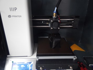
Monoprice Select Mini (PLA filament) 3D printer
For rapid prototyping of new or bespoke parts. Various other 3D printers are available in the Department and STEMLab.
Also available in department:
– Various electronics for flexible experiment design (Keithley multimeters, nanovoltmeters, SRS lock-in, DC power supplies, cryostats and electromagnets)
– Xray Diffraction and Reflectivity (2xD5000, 1xD8, copper source)
– Sample preparation and characterisation (e.g. clean room, ion miller, maskless photolithography, Edwards E306 evaporator, arc furnace, PLD, PVD, metallurgical microscope with camera)


Further characterisation techniques at the Loughborough Materials Characterisation Centre:
- Electron microscopy techniques: SEM, TEM, EDS
- XRF, XPS
- FIB
- Hardness testing
- Differential scanning calorimetry
- Various microscopes
- D2 Xray diffractometer (copper source)
